Sonoscan Imaging Permits Bonded Wafer Rework.
| Author | Foster, Sharon |
| Position | Introducing AW20000 - Product Announcement |
Wafers, which make up part of the circuitry in computer chips, can now be bonded using a new automated bonding system developed by Sonoscan Inc., of Elk Grove Village, Illinois. Bonded wafers use lower power, have faster speeds and can even resist radiation, according to Sonoscan officials. Separating, cleaning and re-bonding defective wafer pairs can bring substantial savings, officials said.
Handling wafers up to 8 inches in diameter, the automated system--known as AW20000--images bonded wafers for particles and other defects between the wafers. The automated system sends sound waves to see inside the wafers to identify any problems. Field reports indicate that the system is especially useful in imaging wafers after initial bonding. This procedure is necessary to insure...
To continue reading
Request your trialCOPYRIGHT GALE, Cengage Learning. All rights reserved.
Subscribers can access the reported version of this case.
You can sign up for a trial and make the most of our service including these benefits.
Why Sign-up to vLex?
-
Over 100 Countries
Search over 120 million documents from over 100 countries including primary and secondary collections of legislation, case law, regulations, practical law, news, forms and contracts, books, journals, and more.
-
Thousands of Data Sources
Updated daily, vLex brings together legal information from over 750 publishing partners, providing access to over 2,500 legal and news sources from the world’s leading publishers.
-
Find What You Need, Quickly
Advanced A.I. technology developed exclusively by vLex editorially enriches legal information to make it accessible, with instant translation into 14 languages for enhanced discoverability and comparative research.
-
Over 2 million registered users
Founded over 20 years ago, vLex provides a first-class and comprehensive service for lawyers, law firms, government departments, and law schools around the world.
Subscribers are able to see a list of all the cited cases and legislation of a document.
You can sign up for a trial and make the most of our service including these benefits.
Why Sign-up to vLex?
-
Over 100 Countries
Search over 120 million documents from over 100 countries including primary and secondary collections of legislation, case law, regulations, practical law, news, forms and contracts, books, journals, and more.
-
Thousands of Data Sources
Updated daily, vLex brings together legal information from over 750 publishing partners, providing access to over 2,500 legal and news sources from the world’s leading publishers.
-
Find What You Need, Quickly
Advanced A.I. technology developed exclusively by vLex editorially enriches legal information to make it accessible, with instant translation into 14 languages for enhanced discoverability and comparative research.
-
Over 2 million registered users
Founded over 20 years ago, vLex provides a first-class and comprehensive service for lawyers, law firms, government departments, and law schools around the world.
Subscribers are able to see a list of all the documents that have cited the case.
You can sign up for a trial and make the most of our service including these benefits.
Why Sign-up to vLex?
-
Over 100 Countries
Search over 120 million documents from over 100 countries including primary and secondary collections of legislation, case law, regulations, practical law, news, forms and contracts, books, journals, and more.
-
Thousands of Data Sources
Updated daily, vLex brings together legal information from over 750 publishing partners, providing access to over 2,500 legal and news sources from the world’s leading publishers.
-
Find What You Need, Quickly
Advanced A.I. technology developed exclusively by vLex editorially enriches legal information to make it accessible, with instant translation into 14 languages for enhanced discoverability and comparative research.
-
Over 2 million registered users
Founded over 20 years ago, vLex provides a first-class and comprehensive service for lawyers, law firms, government departments, and law schools around the world.
Subscribers are able to see the revised versions of legislation with amendments.
You can sign up for a trial and make the most of our service including these benefits.
Why Sign-up to vLex?
-
Over 100 Countries
Search over 120 million documents from over 100 countries including primary and secondary collections of legislation, case law, regulations, practical law, news, forms and contracts, books, journals, and more.
-
Thousands of Data Sources
Updated daily, vLex brings together legal information from over 750 publishing partners, providing access to over 2,500 legal and news sources from the world’s leading publishers.
-
Find What You Need, Quickly
Advanced A.I. technology developed exclusively by vLex editorially enriches legal information to make it accessible, with instant translation into 14 languages for enhanced discoverability and comparative research.
-
Over 2 million registered users
Founded over 20 years ago, vLex provides a first-class and comprehensive service for lawyers, law firms, government departments, and law schools around the world.
Subscribers are able to see any amendments made to the case.
You can sign up for a trial and make the most of our service including these benefits.
Why Sign-up to vLex?
-
Over 100 Countries
Search over 120 million documents from over 100 countries including primary and secondary collections of legislation, case law, regulations, practical law, news, forms and contracts, books, journals, and more.
-
Thousands of Data Sources
Updated daily, vLex brings together legal information from over 750 publishing partners, providing access to over 2,500 legal and news sources from the world’s leading publishers.
-
Find What You Need, Quickly
Advanced A.I. technology developed exclusively by vLex editorially enriches legal information to make it accessible, with instant translation into 14 languages for enhanced discoverability and comparative research.
-
Over 2 million registered users
Founded over 20 years ago, vLex provides a first-class and comprehensive service for lawyers, law firms, government departments, and law schools around the world.
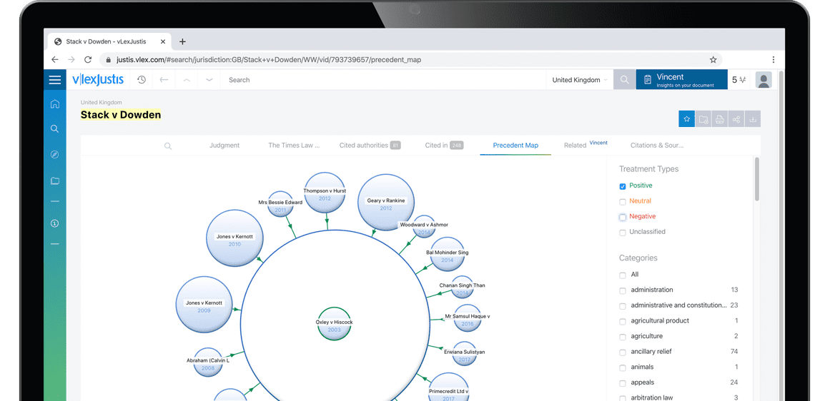
Subscribers are able to see a visualisation of a case and its relationships to other cases. An alternative to lists of cases, the Precedent Map makes it easier to establish which ones may be of most relevance to your research and prioritise further reading. You also get a useful overview of how the case was received.
Why Sign-up to vLex?
-
Over 100 Countries
Search over 120 million documents from over 100 countries including primary and secondary collections of legislation, case law, regulations, practical law, news, forms and contracts, books, journals, and more.
-
Thousands of Data Sources
Updated daily, vLex brings together legal information from over 750 publishing partners, providing access to over 2,500 legal and news sources from the world’s leading publishers.
-
Find What You Need, Quickly
Advanced A.I. technology developed exclusively by vLex editorially enriches legal information to make it accessible, with instant translation into 14 languages for enhanced discoverability and comparative research.
-
Over 2 million registered users
Founded over 20 years ago, vLex provides a first-class and comprehensive service for lawyers, law firms, government departments, and law schools around the world.
Subscribers are able to see the list of results connected to your document through the topics and citations Vincent found.
You can sign up for a trial and make the most of our service including these benefits.
Why Sign-up to vLex?
-
Over 100 Countries
Search over 120 million documents from over 100 countries including primary and secondary collections of legislation, case law, regulations, practical law, news, forms and contracts, books, journals, and more.
-
Thousands of Data Sources
Updated daily, vLex brings together legal information from over 750 publishing partners, providing access to over 2,500 legal and news sources from the world’s leading publishers.
-
Find What You Need, Quickly
Advanced A.I. technology developed exclusively by vLex editorially enriches legal information to make it accessible, with instant translation into 14 languages for enhanced discoverability and comparative research.
-
Over 2 million registered users
Founded over 20 years ago, vLex provides a first-class and comprehensive service for lawyers, law firms, government departments, and law schools around the world.