Electron beams boost nanotechnology.
| Position | Miniaturization - Brief Article |
NASA's Jet Propulsion Laboratory (JPL), Pasadena, Calif., has acquired one of the world's finest electron beam lithography systems, one that will allow researchers to work on the submolecular scale. For NASA, this means breakthroughs in miniaturization that could lead to significant reductions in mass and cost of spacecraft to took for traces of life on distant planets. For researchers, it means access to one of just three such systems in the world, and the only one in the public sector devoted to pure research for building the nanoscale devices of the future.
Operated in the Microdevices Laboratory at JPL, it provides a tool for delving into the realm of nanotechnology, where the individual molecules become accessible to electronic probing. "The E-Beam lithography system will allow researchers to work at the equivalent level of nature's biological building blocks, by allowing them to create and research technologies at the cellular and subcellular level," notes Paul Maker, manager of JPL's Electron Beam Lithography Laboratory. (Lithography is the process of printing a pattern onto a surface, such as a silicon chip or a high-resolution film.)
"The E-Beam lithography system is like a very fast, very high-resolution camera, but instead of exposing photo-sensitive film to light, a thin layer of electron-sensitive material is exposed to electrons. Instead of using a shutter that imprints the whole image at once, an intense electron beam focused to a tiny spot is rastered [scanned] over the chip like the beam that...
To continue reading
Request your trialCOPYRIGHT GALE, Cengage Learning. All rights reserved.
Subscribers can access the reported version of this case.
You can sign up for a trial and make the most of our service including these benefits.
Why Sign-up to vLex?
-
Over 100 Countries
Search over 120 million documents from over 100 countries including primary and secondary collections of legislation, case law, regulations, practical law, news, forms and contracts, books, journals, and more.
-
Thousands of Data Sources
Updated daily, vLex brings together legal information from over 750 publishing partners, providing access to over 2,500 legal and news sources from the world’s leading publishers.
-
Find What You Need, Quickly
Advanced A.I. technology developed exclusively by vLex editorially enriches legal information to make it accessible, with instant translation into 14 languages for enhanced discoverability and comparative research.
-
Over 2 million registered users
Founded over 20 years ago, vLex provides a first-class and comprehensive service for lawyers, law firms, government departments, and law schools around the world.
Subscribers are able to see a list of all the cited cases and legislation of a document.
You can sign up for a trial and make the most of our service including these benefits.
Why Sign-up to vLex?
-
Over 100 Countries
Search over 120 million documents from over 100 countries including primary and secondary collections of legislation, case law, regulations, practical law, news, forms and contracts, books, journals, and more.
-
Thousands of Data Sources
Updated daily, vLex brings together legal information from over 750 publishing partners, providing access to over 2,500 legal and news sources from the world’s leading publishers.
-
Find What You Need, Quickly
Advanced A.I. technology developed exclusively by vLex editorially enriches legal information to make it accessible, with instant translation into 14 languages for enhanced discoverability and comparative research.
-
Over 2 million registered users
Founded over 20 years ago, vLex provides a first-class and comprehensive service for lawyers, law firms, government departments, and law schools around the world.
Subscribers are able to see a list of all the documents that have cited the case.
You can sign up for a trial and make the most of our service including these benefits.
Why Sign-up to vLex?
-
Over 100 Countries
Search over 120 million documents from over 100 countries including primary and secondary collections of legislation, case law, regulations, practical law, news, forms and contracts, books, journals, and more.
-
Thousands of Data Sources
Updated daily, vLex brings together legal information from over 750 publishing partners, providing access to over 2,500 legal and news sources from the world’s leading publishers.
-
Find What You Need, Quickly
Advanced A.I. technology developed exclusively by vLex editorially enriches legal information to make it accessible, with instant translation into 14 languages for enhanced discoverability and comparative research.
-
Over 2 million registered users
Founded over 20 years ago, vLex provides a first-class and comprehensive service for lawyers, law firms, government departments, and law schools around the world.
Subscribers are able to see the revised versions of legislation with amendments.
You can sign up for a trial and make the most of our service including these benefits.
Why Sign-up to vLex?
-
Over 100 Countries
Search over 120 million documents from over 100 countries including primary and secondary collections of legislation, case law, regulations, practical law, news, forms and contracts, books, journals, and more.
-
Thousands of Data Sources
Updated daily, vLex brings together legal information from over 750 publishing partners, providing access to over 2,500 legal and news sources from the world’s leading publishers.
-
Find What You Need, Quickly
Advanced A.I. technology developed exclusively by vLex editorially enriches legal information to make it accessible, with instant translation into 14 languages for enhanced discoverability and comparative research.
-
Over 2 million registered users
Founded over 20 years ago, vLex provides a first-class and comprehensive service for lawyers, law firms, government departments, and law schools around the world.
Subscribers are able to see any amendments made to the case.
You can sign up for a trial and make the most of our service including these benefits.
Why Sign-up to vLex?
-
Over 100 Countries
Search over 120 million documents from over 100 countries including primary and secondary collections of legislation, case law, regulations, practical law, news, forms and contracts, books, journals, and more.
-
Thousands of Data Sources
Updated daily, vLex brings together legal information from over 750 publishing partners, providing access to over 2,500 legal and news sources from the world’s leading publishers.
-
Find What You Need, Quickly
Advanced A.I. technology developed exclusively by vLex editorially enriches legal information to make it accessible, with instant translation into 14 languages for enhanced discoverability and comparative research.
-
Over 2 million registered users
Founded over 20 years ago, vLex provides a first-class and comprehensive service for lawyers, law firms, government departments, and law schools around the world.
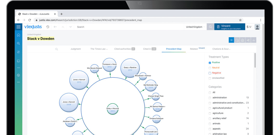
Subscribers are able to see a visualisation of a case and its relationships to other cases. An alternative to lists of cases, the Precedent Map makes it easier to establish which ones may be of most relevance to your research and prioritise further reading. You also get a useful overview of how the case was received.
Why Sign-up to vLex?
-
Over 100 Countries
Search over 120 million documents from over 100 countries including primary and secondary collections of legislation, case law, regulations, practical law, news, forms and contracts, books, journals, and more.
-
Thousands of Data Sources
Updated daily, vLex brings together legal information from over 750 publishing partners, providing access to over 2,500 legal and news sources from the world’s leading publishers.
-
Find What You Need, Quickly
Advanced A.I. technology developed exclusively by vLex editorially enriches legal information to make it accessible, with instant translation into 14 languages for enhanced discoverability and comparative research.
-
Over 2 million registered users
Founded over 20 years ago, vLex provides a first-class and comprehensive service for lawyers, law firms, government departments, and law schools around the world.
Subscribers are able to see the list of results connected to your document through the topics and citations Vincent found.
You can sign up for a trial and make the most of our service including these benefits.
Why Sign-up to vLex?
-
Over 100 Countries
Search over 120 million documents from over 100 countries including primary and secondary collections of legislation, case law, regulations, practical law, news, forms and contracts, books, journals, and more.
-
Thousands of Data Sources
Updated daily, vLex brings together legal information from over 750 publishing partners, providing access to over 2,500 legal and news sources from the world’s leading publishers.
-
Find What You Need, Quickly
Advanced A.I. technology developed exclusively by vLex editorially enriches legal information to make it accessible, with instant translation into 14 languages for enhanced discoverability and comparative research.
-
Over 2 million registered users
Founded over 20 years ago, vLex provides a first-class and comprehensive service for lawyers, law firms, government departments, and law schools around the world.